
CPU/GPU/TPU/NPU…What does XPU mean?
CPU / GPU / TPU / NPU …What does XPU mean?
In this era, technology is changing with each passing day, concepts such as the Internet of Things, artificial intelligence, and deep learning are everywhere, and various chip terms GPU, TPU, NPU, and DPU are emerging one after another… What the hell is it? What is the relationship with the CPU?
HW has released a new Mate phone, which has an NPU called inside. It sounds amazing. What is this? It is an artificial intelligence processor.
What is an artificial intelligence processor? What’s the difference between it and CPU? What’s the difference between it and GPU? Don’t you bring a PU?
This article will give you some popular science on these so-called “XPUs”!
CPU
The CPU (Central Processing Unit) is the “brain” of the machine, and it is also the “commander-in-chief ” who lays out strategies, issues orders, and controls actions .
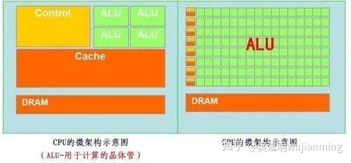
The CPU structure mainly includes an arithmetic and Logic Unit, a control unit (CU, Control Unit), a register (Register), a cache (Cache), and a bus for communication data, control and status.
Simply put, it is: computing unit, control unit and storage unit , the architecture is shown in the figure below:
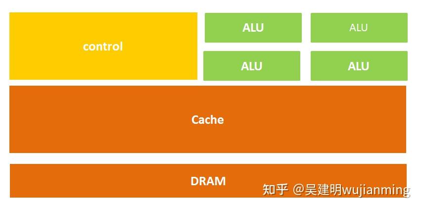
Figure: CPU micro architecture diagram
Another way to express:
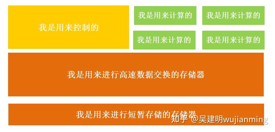
Figure: CPU micro architecture diagram (change)
That’s probably what it means.
It is also easy to understand literally. The calculation unit mainly performs arithmetic operations, shifting and other operations, as well as address operations and conversion; the storage unit is mainly used to save data and instructions generated in the calculation; the control unit decodes the instructions and issues control signals to complete the various operations to be performed by each instruction.
Therefore, the process of an instruction being executed in the CPU is as follows: after reading the instruction, it is sent to the controller (yellow area) through the instruction bus for decoding, and a corresponding operation control signal is sent; then the operator (green area) calculates the data according to the operation instructions, and stores the obtained data into the data buffer (large blocks of orange areas) through the data bus. The process is shown in the figure below:
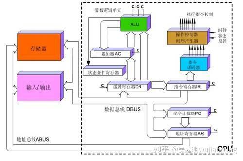
Figure: CPU execution instruction diagram
The CPU follows the von Neumann architecture , and its core is: stored programs and executed sequentially. In this structural diagram, the area occupied by the green area responsible for the calculation seems to be too small, while the cache cache of the orange area and the control unit of the yellow area occupy a lot of space.
Because the CPU architecture requires a lot of space to place the storage unit (orange part) and the control unit (yellow part) , in contrast, the computing unit (green part) only accounts for a small part, so it is extremely limited in large-scale parallel computing capabilities and is better at logical control.
In addition, because following the von Neumann architecture (storage programs, executed sequentially), the CPU is like a scheming butler, and it always does what people command it step by step. But as people’s demand for larger scale and faster processing speeds increases, the butler gradually becomes a little overwhelmed.
So, everyone wondered whether multiple processors can be placed on the same chip and worked together, so that the efficiency will be improved?
That’s right, the GPU was born.
GPU
Before formally explaining GPU, let’s talk about a concept – parallel computing.
Parallel Computing refers to an effective means to use multiple computing resources to solve computing problems at the same time and improve the computing speed and processing capabilities of computer systems. The basic idea is to use multiple processors to solve the same problem together, and the solved problem is broken down into several parts, each part being calculated in parallel by an independent processor.
Parallel computing can be divided into parallelism in time and parallelism in space .
Parallelism in time refers to assembly line technology. For example, when a factory produces food, it is divided into four steps: cleaning – disinfection – cutting – packaging.
If the assembly line is not used, the next food will be processed only after one food completes the above four steps, which will take time and affect efficiency. Using assembly line technology, four foods are processed simultaneously. This is the time parallelism in parallel algorithms, starting two or more operations at the same time, greatly improving computing performance.
Figure: Schematic diagram of the assembly line
Parallelism in space refers to the concurrent execution of multiple processors, that is, connecting more than two processors through the network to achieve large-scale problems that can be solved by calculating different parts of the same task at the same time, or a single processor cannot solve.
For example, Xiao Li is preparing to plant three trees on Arbor Day. If Xiao Li takes 6 hours to complete the task, on Arbor Day, he called his good friends Xiaohong and Xiao Wang. The three of them started digging pits and planting trees at the same time. After 2 hours, each completed a tree planting task. This is the parallelism of space in the parallel algorithm, which divides a large task into multiple same subtasks to speed up the problem solving speed.
So, if the CPU is allowed to perform this tree planting task, it will plant one by one, and it will take 6 hours, but if the GPU is allowed to plant trees, it is equivalent to several people planting them at the same time.
The full name of the GPU is Graphics Processing Unit , which is a graphics processor in Chinese . Just like its name, the GPU was originally a microprocessor that runs drawing operations on personal computers, workstations, game consoles and some mobile devices (such as tablets, smartphones, etc.).
Why are GPUs particularly good at processing image data? This is because every pixel point on the image needs to be processed, and the process and method of each pixel point are very similar, which has become a natural breeding ground for GPUs.
The simple GPU architecture is shown in the figure below:
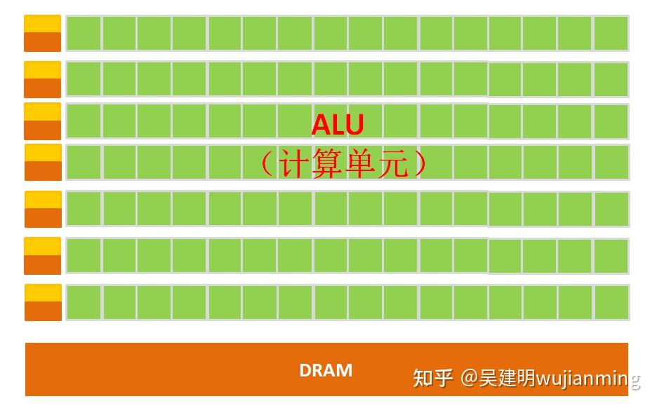
Figure: Schematic diagram of GPU micro architecture
It can be clearly seen from the architecture diagram that the composition of the GPU is relatively simple, with a large number of computing units and ultra-long pipelines, which are particularly suitable for processing a large number of unified data of types.
However, the GPU cannot work alone and must be controlled by the CPU to work . The CPU can act alone to process complex logical operations and different data types. When a large amount of data processing of unified types is required, the GPU can be called for parallel computing.
Note: There are many ALUs and very few cache caches in the GPU. The purpose of cache is not to save the data that needs to be accessed later. This is different from the CPU, but to improve the service of thread threads. If many threads need to access the same data, the cache will merge these accesses and then access the Dram.
Then put the CPU and GPU in the same picture and compare it, and it will be very clear at a glance.
Most of the work of GPUs is computationally expensive, but it has no technical content, and it needs to be repeated many times.
To borrow the statement of a master on Zhihu, just like if you have a job that requires calculation of addition, subtraction, multiplication and division within a hundred times, the best way is to hire dozens of primary school students to calculate together, one person calculates part of it. Anyway, these calculations do not have much technical content, just physical work; and the CPU is like an old professor, and the integral and differentials can be calculated, which is the salary is high, and an old professor is worth twenty primary school students. If it is Foxconn, which one should I hire?
GPU uses many simple computing units to complete a large number of computing tasks, purely human-sea tactics. This strategy is based on a premise, that is, the work of primary school student A and primary school student B have no dependence on it and are independent of each other.
But one thing needs to be emphasized. Although GPU is born for image processing, through the previous introduction, we can find that there are no components that specifically serve images in structure , but only optimize and adjust the CPU structure. Therefore, now GPU can not only show its skills in the field of image processing, but is also used in scientific computing, password cracking, numerical analysis, massive data processing (sorting, Map-Reduce, etc.), financial analysis and other fields that require large-scale parallel computing.
Therefore, the GPU can also be considered a more general chip.
TPU
As mentioned above, both CPU and GPU are relatively general chips, but there is an old saying: universal tools are never as efficient as special tools.
As people’s computing needs become more and more specialized, people hope that chips can be more in line with their professional needs. At this time, the concept of ASIC (application-specific integrated circuit) was born .
ASIC refers to a special specification integrated circuit customized according to product requirements, designed and manufactured by specific users and specific electronic systems. Of course, this concept is not to be remembered, it is simply customized chips.
Because ASIC is very “specialized” and only does one thing, it will do better in a certain thing than chips such as CPUs and GPUs that can do many things, achieving higher processing speeds and lower energy consumption. But accordingly, the production cost of ASIC is also very high.
TPU (Tensor Processing Unit) is a chip developed by Google specifically to accelerate deep neural network computing capabilities, and it is actually an ASIC.
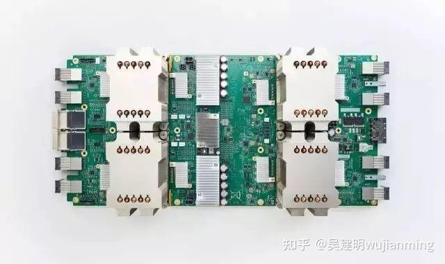
Picture: Google’s second generation TPU
It is difficult for ordinary companies to bear the cost and risks of developing specialized ASIC chips for deep learning, but who is Google, will people lose money?
The more important reason is that many services provided by Google, including Google image search, Google photos, Google cloud vision API, Google Translation and other products and services, all require deep neural networks. Based on Google’s own huge size, developing a specialized chip has the possibility of large-scale application (largely sharing R&D costs).
In this way, it is natural for TPU to enter the historical stage.
It turns out that most of the machine learning and image processing algorithms run on GPU and FPGA (semi-customized chip), but both chips are still a general chip, so they cannot adapt to machine learning algorithms more closely in terms of performance and power consumption. Moreover, Google has always believed that great software will shine even more with the help of great hardware, so Google wondered whether it could make a dedicated chip for machine learning algorithms for a dedicated machine, and TPU was born.
It is said that TPU can provide 15-30x performance improvements and 30-80x efficiency (performance/watt) improvements compared to CPUs and GPUs of the same period. The first generation of TPUs can only do inference and rely on Google Cloud to collect data and generate results in real time. The training process also requires additional resources; the second generation of TPUs can be used to train neural networks and inference.
Why is TPU so awesome in performance?
Google has written several papers and blog posts to explain this reason, so I will only give you some tips here.
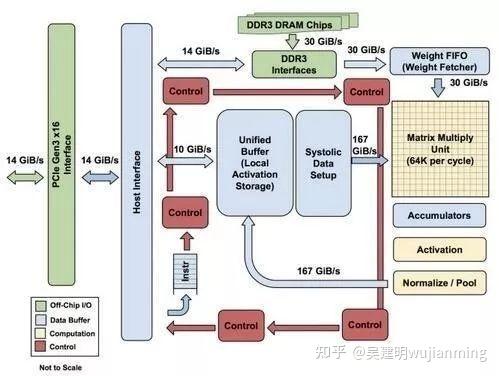
Figure: Block diagram of each TPU module
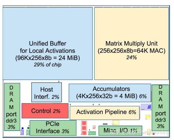
Picture: TPU chip layout diagram
As shown in the figure above, the TPU uses up to 24MB of local memory, 6MB of accumulator memory and memory used to connect with the main processor on the chip, accounting for 37% of the chip area in total (the blue part in the figure).
This means that Google fully realizes that off-chip memory access is the culprit of GPU’s low energy efficiency ratio, so it puts huge memory on the chip at all costs. In contrast, Nvidia’s K80 at the same time only had 8MB of on-chip memory and needed to continuously access off-chip DRAM.
In addition, the high performance of TPU also comes from tolerance for low computing accuracy. Research results show that the algorithm accuracy loss caused by low-precision computing is very small, but it can bring huge convenience in hardware implementation, including lower power consumption, faster speed, smaller chip area, and smaller memory bandwidth requirements… The TPU uses 8-bit low-precision computing.
For more information, please read Google’s papers.
So far, TPU has actually done a lot of things, such as the machine learning artificial intelligence system RankBrain, which is used to help Google process search results and provide users with more relevant search results; there is also the Street View, which is used to improve the accuracy of maps and navigation; of course, there is also the computer program AlphaGo, which plays Go!
NPU
I believe everyone has a certain understanding of these so-called “XPU” routines.
The so-called NPU (Neural network Processing Unit) is a neural network processor . As the name suggests, this guy wants to use circuits to simulate human neurons and synaptic structures!
How to imitate? Then we have to first look at the neural structure of humans – the biological neural network is composed of several artificial neuron nodes interconnected, and neurons are connected by synapses, which record the connection between neurons.
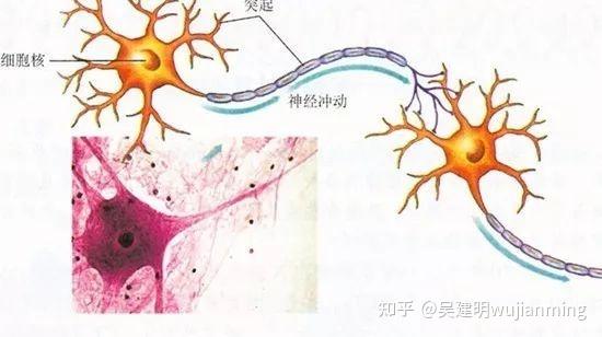
If you want to use circuits to imitate human neurons, you have to abstract each neuron into an excitation function, and the input of the function is determined by the output of the neuron connected to it and the synapses connecting the neurons.
In order to express specific knowledge, users usually need to adjust the synaptic values, the topological structure of the network in artificial neural networks, etc. (through certain specific algorithms). This process is called “learning.”
After learning, artificial neural networks can solve specific problems through the learned knowledge.
At this time, I don’t know if you have found any problems – it turns out that since the basic operations of deep learning are the processing of neurons and synapses, the traditional processor instruction set (including x86 and ARM, etc.) was developed for general computing. The basic operations are arithmetic operations (addition, subtraction, multiplication and division) and logical operations (and or non), and often hundreds or even thousands of instructions are required to complete the processing of a neuron, and the processing efficiency of deep learning is not high.
At this time, we must find a different approach – break through the classic von Neumann structure!
Storage and processing in neural networks are integrated and are both reflected through synaptic weights. In the von Neumann structure, storage and processing are separated and implemented by memory and arithmetic respectively. There are huge differences between the two. When using existing classic computers based on von Neumann structures (such as X86 processors and NVIDIA GPUs) to run neural network applications, they are inevitably subject to the constraints of storage and processing of separate structures, thus affecting efficiency. This is one of the reasons why professional chips specifically target artificial intelligence can have certain innate advantages over traditional chips.
Typical representatives of NPUs include domestic Cambrian chips and IBM’s TrueNorth . Taking the Cambrian in China as an example, the DianNaoYu instruction directly faces the processing of large-scale neurons and synapses. One instruction can complete the processing of a group of neurons and provide a series of special support for the transmission of neurons and synaptic data on the chip.
To put it in terms of numbers, CPUs and GPUs will have a performance or energy consumption ratio gap of more than 100 times compared to NPUs. Take the DianNao paper jointly published by the Cambrian team in the past and Inria as an example. DianNao is a single-core processor with a main frequency of 0.98GHz, and a peak performance of 452 billion neural network basic operations per second. The power consumption under the 65nm process is 0.485W and an area of 3.02 square millimeters mm.
The Kirin 970 chip used in Huawei mate 10 integrates Cambrian NPU, so it can realize the so-called photo optimization function, ensuring that the phone will not be stuck after using it for a long time (of course, you have to use it to know if there is such a good publicity).
PS. Although Zhongxing Microelectronics’ “Starlight Intelligence One” is known as an NPU, it is actually just DSP. It only supports forward network computing and cannot support neural network training.
Based on the above knowledge, it is easier to understand BPU and DPU.
BPU (Brain Processing Unit) is an embedded artificial intelligence processor architecture proposed by Horizon Technology . The first generation is the Gaussian architecture, the second generation is the Bernoulli architecture, and the third generation is the Bayesian architecture. Horizon has designed the first generation of Gaussian architecture and jointly launched the ADAS system (Advanced Driver Assistance System) with Intel at the 2017 CES show.
DPU (Deep learning Processing Unit, namely, deep learning processor) was first proposed by domestic Shenjian Technology . It is based on Xilinx’s reconfigurable FPGA chip, designed a dedicated deep learning processing unit (can design parallel and efficient multiplier and logic circuit based on existing logic units, which belongs to the IP category), and abstracts customized instruction sets and compilers (rather than using OpenCL), thereby achieving rapid development and product iteration. In fact, the DPU proposed by Shenjian belongs to semi-customized FPGAs.
It is said that every 18 days, an additional XPU will appear in the integrated circuit field until the 26 letters are used up.
This is nicknamed the XPU version of Moore’s Law in the AI era.
According to incomplete statistics, those that have been used up are:
APU — Accelerated Processing Unit, Accelerated Processing Unit , AMD launched an accelerated image processing chip product.
BPU — Brain Processing Unit , an embedded processor architecture dominated by Horizon.
CPU — Central Processing Unit Central Processing Unit , currently the mainstream product of PC core.
DPU — Deep learning Processing Unit, a deep learning processor , first proposed by domestic Shenjian Technology; it also says that there is the Dataflow Processing Unit data stream processor, the AI architecture proposed by Wave Computing; Data storage Processing Unit, an intelligent solid-state hard drive processor of Shenzhen Dapuwei.
FPU — Floating Processing Unit Floating point computing unit , floating point computing module in general processors.
GPU — Graphics Processing Unit, graphics processor , adopts a multi-threaded SIMD architecture, and is born for graphics processing.
HPU — Holographics Processing Unit Holographic image processor , a holographic computing chip and device produced by Microsoft.
IPU — Intelligence Processing Unit , an AI processor product produced by Graphcore, a company invested by Deep Mind.
MPU/MCU — Microprocessor/Micro controller Unit , microprocessor/micro controller, is generally used for low-computing applications RISC computer architecture products, such as ARM-M series processors.
NPU — Neural Network Processing Unit , a general term for neural network processors, new processors based on neural network algorithms and acceleration, such as the diannao series produced by the Institute of Computing, Chinese Academy of Sciences/Cambrian.
RPU — Radio Processing Unit, radio processor , a collection of Wifi/Bluetooth/FM/processor launched by Imagination Technologies is a monolithic processor.
TPU — Tensor Processing Unit tensor processor , a dedicated processor for accelerating artificial intelligence algorithms launched by Google. Currently, the first generation of TPU is aimed at Inference and the second generation is aimed at training.
VPU — Vector Processing Unit vector processor , Intel acquired Movidius to accelerate computing core of image processing and artificial intelligence dedicated chips.
WPU — Wearable Processing Unit, a wearable processor , a wearable system-on-chip product launched by Ineda Systems, including GPU/MIPS CPU and other IPs.
XPU — FPGA intelligent cloud acceleration released by Baidu and Xilinx at the 2017 Hotchips Conference , including 256 cores.
ZPU — Zylin Processing Unit, a 32-bit open source processor launched by Norway’s Zylin.
When the 26 letters are used up, XXPU, XXXPU will appear, and the naming world will be occupied at a faster speed.
I believe you have also gained a preliminary understanding of the concepts of these XPUs.